| Single-Sided PCB | One conductive copper layer bonded to an insulating substrate, with components generally mounted on the opposite side. | 1 copper layer | Glass-reinforced epoxy laminate, paper-based phenolic laminate, copper foil, and solder mask. | Electrical signals travel between component pads through copper traces on one side of the board. | Low manufacturing cost, simple layout, fast production, and easy inspection. | Basic power supplies, LED lighting, simple timers, calculators, and low-complexity consumer devices. | Routing space is limited, and crossing signal paths may require jumpers or additional wiring. |
| Double-Sided PCB | Conductive copper layers are present on both sides of the insulating core and are connected through plated holes or vias. | 2 copper layers | Glass-reinforced epoxy laminate, copper foil, plated-through holes, solder mask, and surface finish. | Signals can move between the two copper layers through vias, allowing traces to cross more efficiently. | Higher routing density than single-sided boards while remaining relatively economical. | Industrial controls, instrumentation, automotive modules, household appliances, and medium-complexity electronics. | Via placement, return-current paths, electromagnetic interference, and component clearance must be managed carefully. |
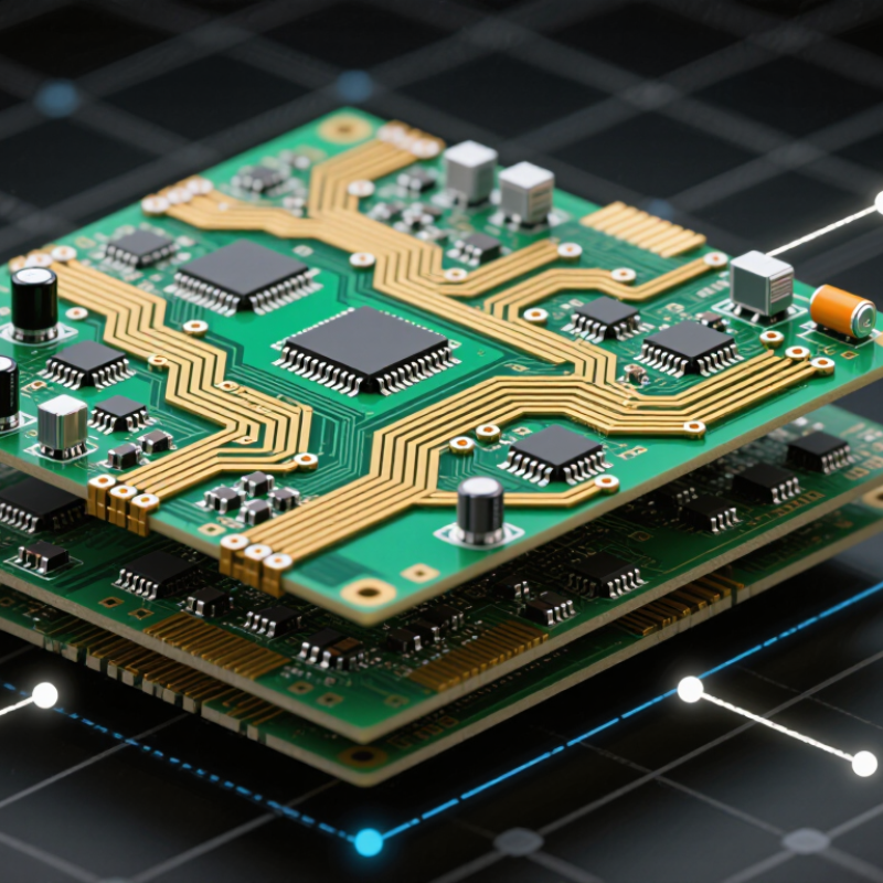
| Multilayer PCB | Several copper layers are separated by insulating dielectric layers and laminated into one board. | 4 to 30+ layers | Glass-reinforced epoxy laminate, low-loss dielectric materials, copper foil, prepreg, and plated vias. | Different layers can be assigned to signals, power, and ground, while vias provide interconnection between selected layers. | High circuit density, controlled impedance, improved power distribution, and reduced board size. | Computers, networking equipment, medical instruments, industrial controllers, and complex embedded systems. | Stack-up design, thermal management, fabrication tolerances, signal integrity, and higher manufacturing cost are critical. |
| Rigid PCB | A fixed, non-bendable board made from a solid laminate structure. | 1 to 30+ layers | Glass-reinforced epoxy laminate, high-temperature laminates, copper, solder mask, and protective surface finishes. | Components are mounted on a stable platform, and copper patterns provide permanent electrical pathways. | Mechanical strength, dimensional stability, reliable assembly, and broad material availability. | Control panels, computers, appliances, measurement equipment, power electronics, and vehicle electronics. | Board outline, mounting holes, vibration, thermal expansion, and component placement must match the enclosure. |
| Flexible PCB | Thin conductive layers are formed on a bendable polymer film instead of a rigid laminate. | 1 to 6+ layers | Polyimide or similar flexible film, rolled or electrodeposited copper, flexible coverlay, and stiffeners where needed. | Flexible copper traces carry signals while the circuit bends or folds within its specified bend radius. | Light weight, reduced wiring, space saving, and improved resistance to repeated movement when correctly designed. | Displays, cameras, wearable devices, compact sensors, printers, and moving mechanical assemblies. | Minimum bend radius, bend-cycle life, copper grain direction, strain relief, and connector reinforcement are essential. |
| Rigid-Flex PCB | Rigid board sections are permanently integrated with flexible circuit sections in a single assembled structure. | Multiple rigid and flex layers | Rigid epoxy laminate, flexible polyimide, copper, coverlay, prepreg, and mechanically reinforced transition areas. | Rigid zones support components, while flexible zones fold to connect separate sections without cable harnesses. | Fewer connectors, lower assembly volume, improved reliability, and better three-dimensional packaging. | High-reliability instruments, aerospace systems, surgical equipment, compact industrial devices, and portable electronics. | Transition geometry, dynamic versus static bending, heat during assembly, and repairability require careful planning. |
| HDI PCB | A high-density multilayer board using fine traces, small pads, microvias, and sometimes sequentially built layers. | Usually 4+ layers | Fine-line laminate materials, copper foil, laser-drilled microvias, and low-loss dielectric materials when required. | Microvias and fine routing features connect densely packed components across short interconnection paths. | Compact form factor, improved electrical performance, and high component density. | Smart devices, compact computing products, high-density modules, miniature medical equipment, and advanced sensors. | Registration accuracy, via reliability, trace width control, thermal constraints, and specialized fabrication capability are important. |
| Metal-Core PCB | A conductive metal base supports the circuit and transfers heat away from components through a dielectric insulation layer. | Usually 1 to 2 copper layers | Aluminum or copper base, thermally conductive dielectric, copper circuit layer, and solder mask. | Electrical current follows the copper circuitry while heat flows through the dielectric into the metal core and then to a heatsink or enclosure. | Excellent heat spreading, improved thermal stability, and reduced need for separate thermal hardware. | High-power LED lighting, motor controllers, power converters, automotive lighting, and industrial power modules. | Thermal resistance, electrical isolation, coefficient of thermal expansion, and mechanical fastening must be evaluated. |
| High-Frequency PCB | A board designed with controlled electrical properties for signals operating at radio-frequency or microwave ranges. | 2 to 12+ layers | Low-loss laminates, specialized resin systems, copper foil, and materials with controlled dielectric constant and loss tangent. | Controlled-impedance traces guide high-speed signals while minimizing reflection, attenuation, and unwanted coupling. | Lower signal loss, predictable transmission behavior, and improved performance at high frequencies. | Wireless communication equipment, radar modules, satellite systems, test instruments, and high-speed data links. | Dielectric properties, trace geometry, surface roughness, connector transitions, grounding, and electromagnetic shielding are critical. |
| Ceramic PCB | A circuit board using a ceramic substrate that provides electrical insulation and strong thermal performance. | 1 to 10+ layers | Alumina, aluminum nitride, or other technical ceramics with thick-film, thin-film, or bonded copper conductors. | Conductive patterns carry current while the ceramic substrate provides insulation, dimensional stability, and heat transfer. | High thermal conductivity, low moisture absorption, low thermal expansion, and strong high-temperature performance. | Power modules, laser systems, high-temperature sensors, microwave assemblies, and demanding industrial electronics. | Brittleness, machining methods, thermal cycling, attachment processes, and comparatively high material cost must be considered. |
| Power PCB | A board engineered with heavy copper, wide conductors, large terminals, and strong thermal and mechanical features. | 1 to 12+ layers | Heavy-copper laminate, metal-core materials, high-temperature dielectric systems, large copper planes, and reinforced terminals. | Wide or thick copper paths carry high current, while planes, vias, and thermal structures distribute heat and reduce electrical losses. | High current capacity, improved heat dissipation, and enhanced electrical and mechanical robustness. | Battery management systems, inverters, motor drives, industrial power supplies, and energy conversion equipment. | Current density, temperature rise, creepage and clearance, copper weight, fault conditions, and thermal cycling are central design factors. |



 © Copyright 2020 Tianjin Tanghaidongyang Valve Co., Ltd. All Rights Reserved.